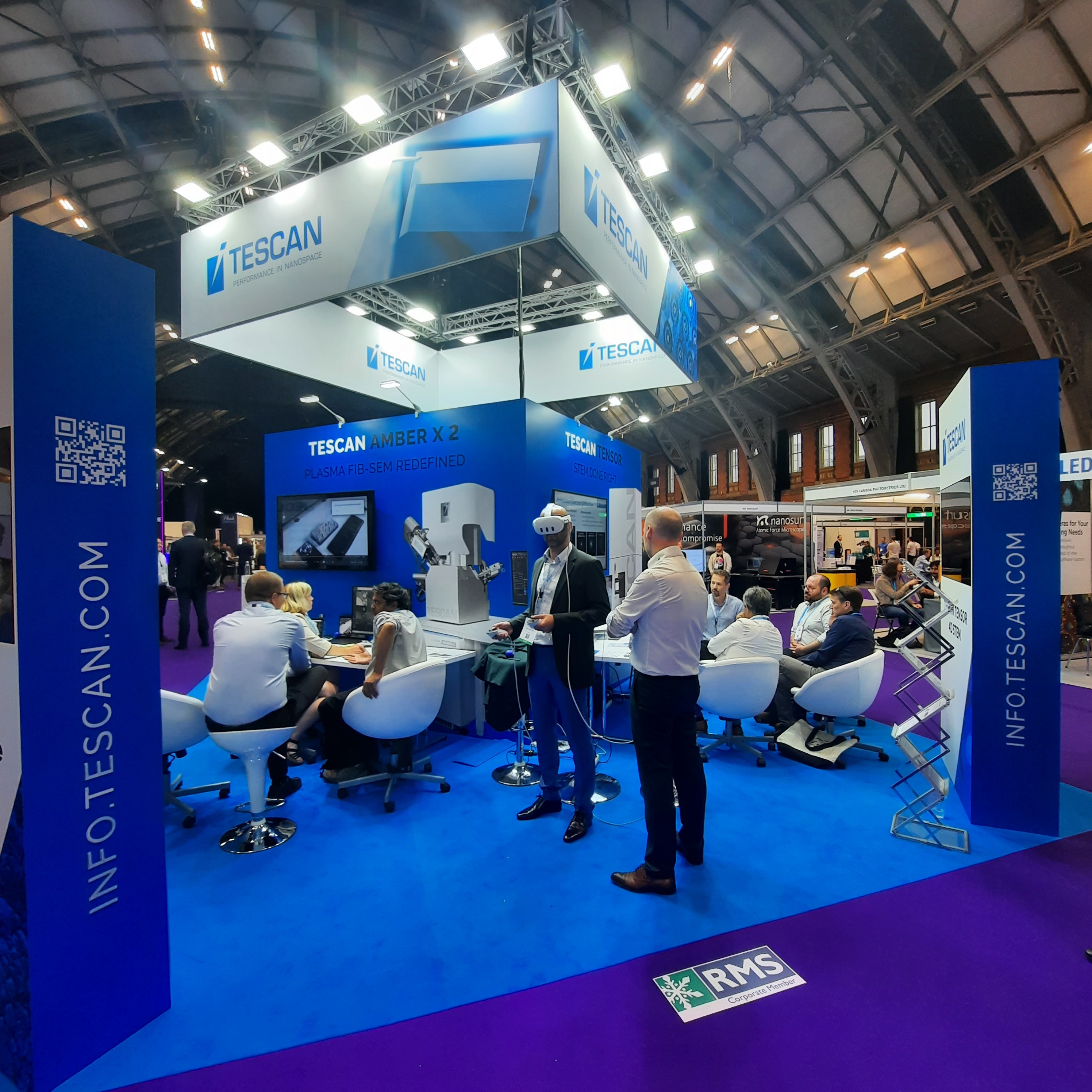
Meet TESCAN at

Microscopy Conference 2025


Join TESCAN for Live Demos, Expert Sessions,

and Innovation at MC 2025 


Booth #15 · Live Demos · Scientific Sessions · New Features

Aug 31 – Sept 4 · Messe Karlsruhe · Germany

Meet us now...
days
hours
:
minutes
:
sec

TESCAN is heading back to MC - as always, ready to connect, share, and inspire.


Visit us at Booth #15 for live demonstrations of our most advanced platforms for electron microscopy, micro-CT, and nanoscale analysis. Whether you're working in R&D, failure analysis, quality control, or academic research, you'll see how TESCAN supports your work through intelligent automation, multimodal characterisation, and user-centered innovation.


Something new is coming to MC - and it starts at TESCAN’s booth.
Stop by, and you’ll see it in a whole new way.

Book a Live Demo


Meet our experts throughout the day and book a personalized, on-screen walkthrough of the latest innovations and workflows we’re showcasing at the event.
DSC05967-perspektiva-02-sytos kopie-2

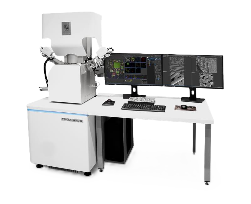
MIRA XR

Ultra-High-Resolution SEM for Fast Materials Analysis

Designed for high-throughput labs, MIRA XR delivers reliable nanoscale imaging with intuitive controls and seamless EDS mapping — ideal for both expert users and shared facilities

x
Register for a demo
x

MIRA XR

AMBERX_2025_Solldesign_RGB_MOTIV9_XCL9_LAYERS_10k kopie

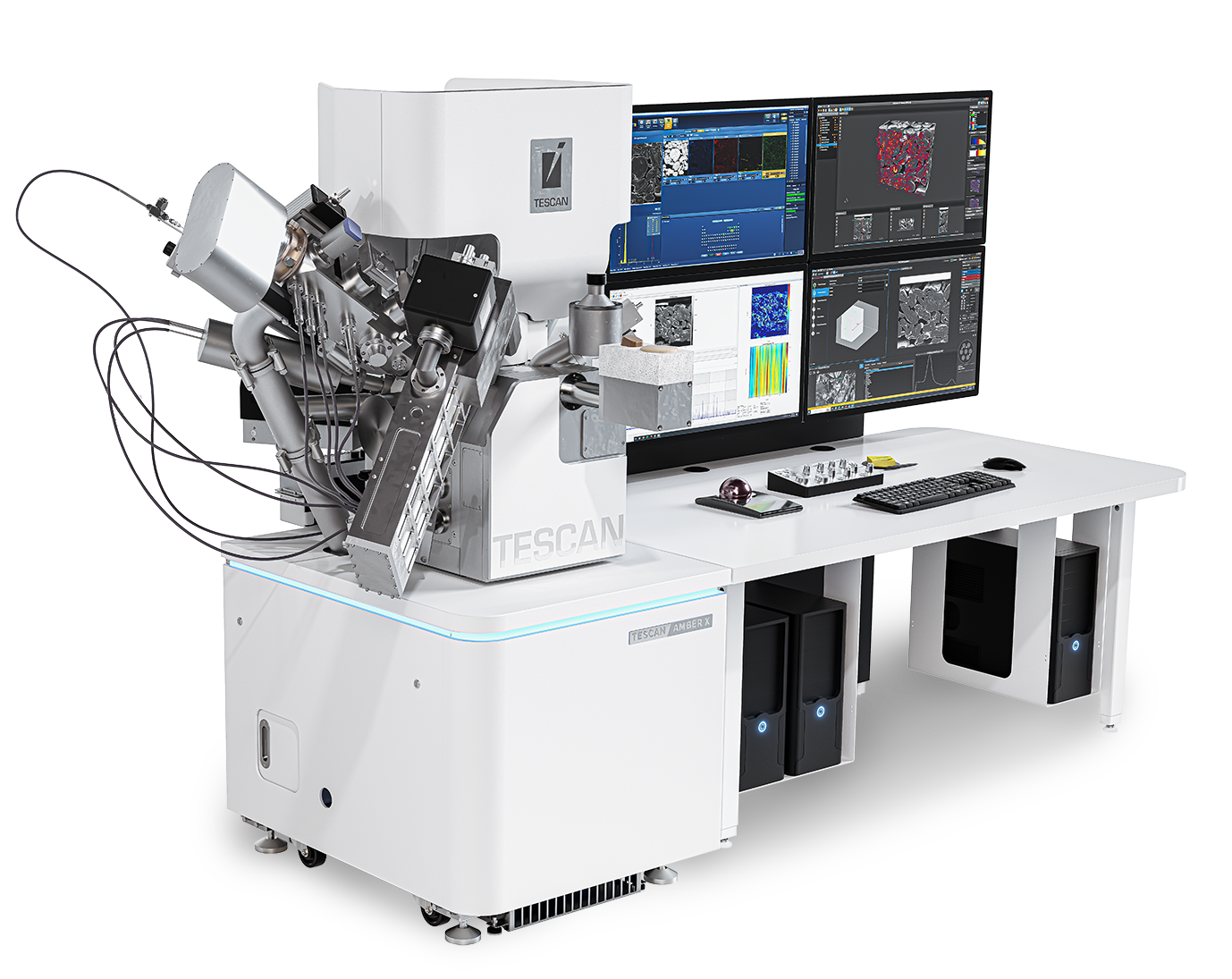
AMBER X 2

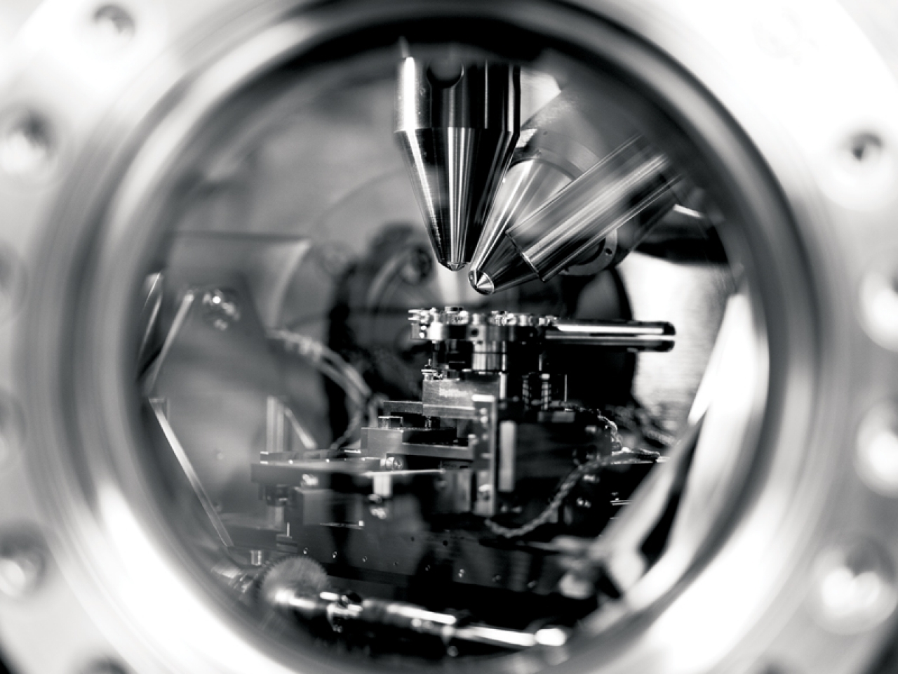
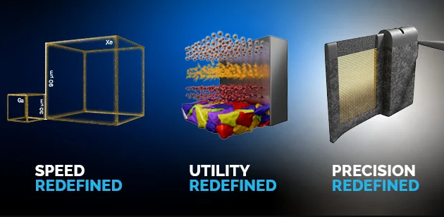
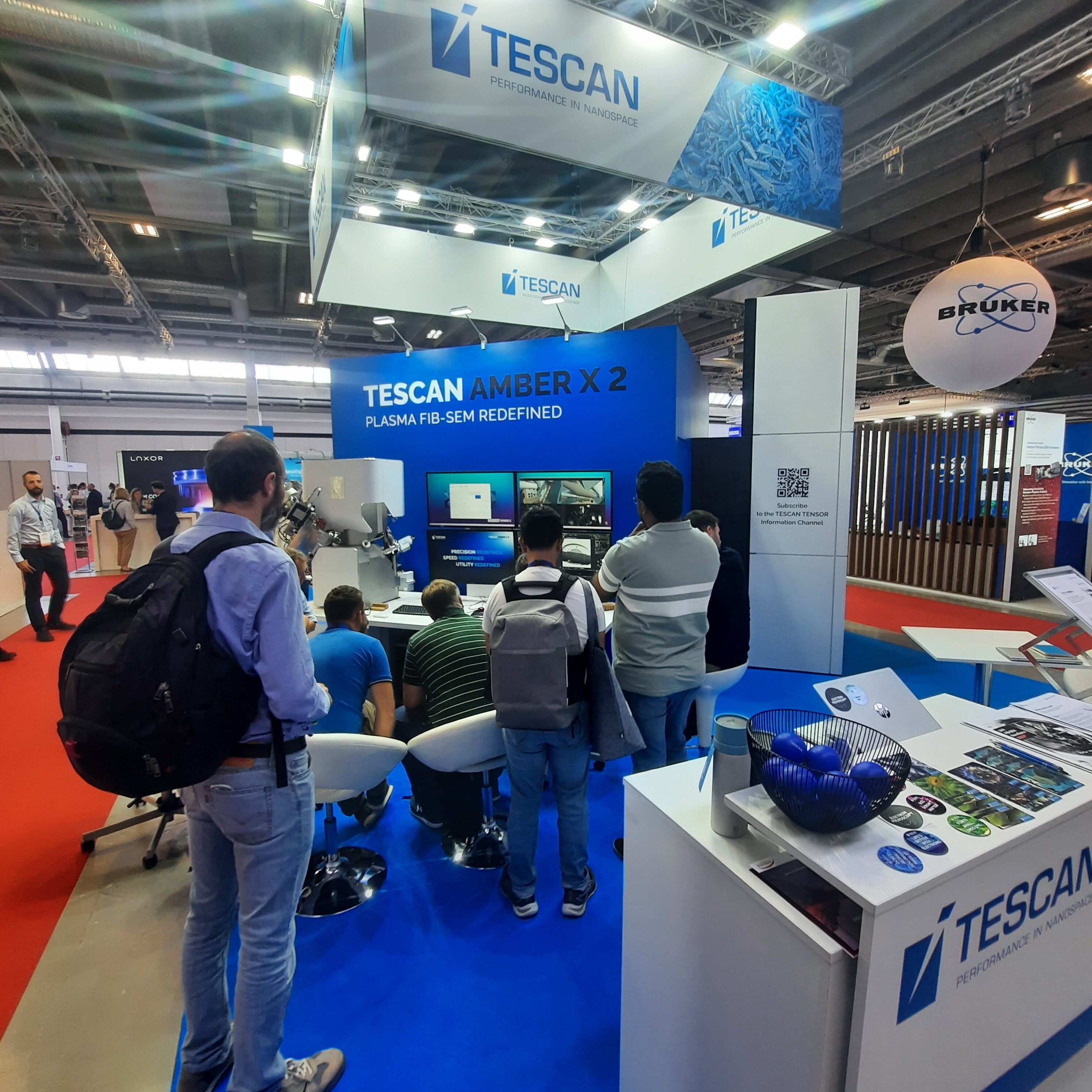
High-Throughput Plasma FIB-SEM for Advanced Applications

3D analysis, TEM prep and delayering — all in one platform. AMBER X 2 combines field-free UHR-SEM and high-current Xe plasma FIB for fast, clean, and artifact-free results across materials and semiconductor workflows
x AMBERX_2025_Solldesign_RGB_MOTIV9_XCL9_LAYERS_10k kopie
Register for a demo
x

AMBER X 2

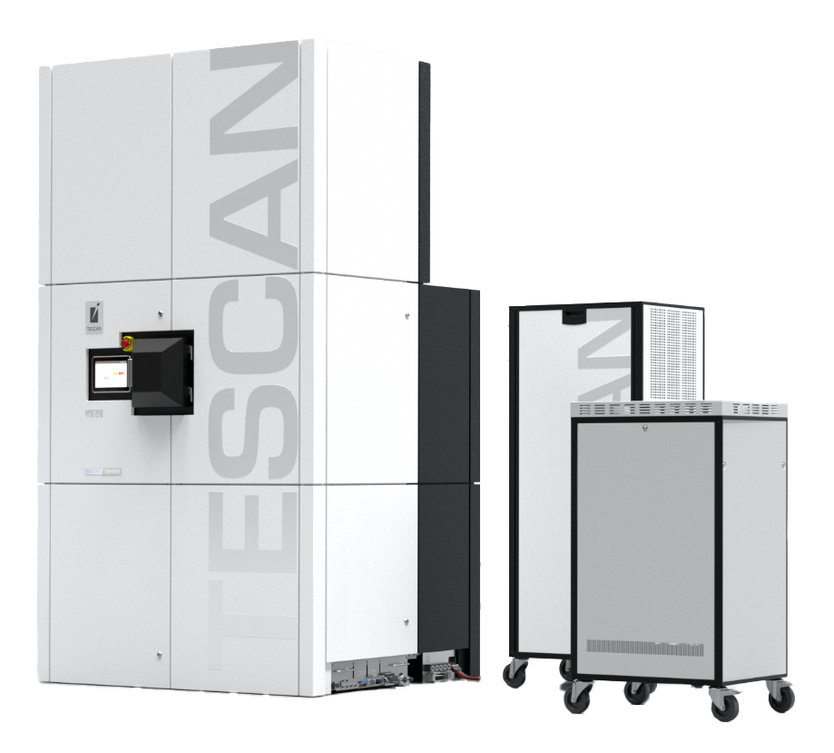
TENSOR with cabinets-2

TENSOR

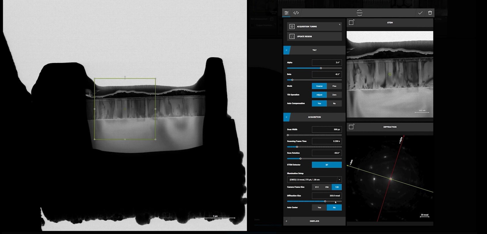
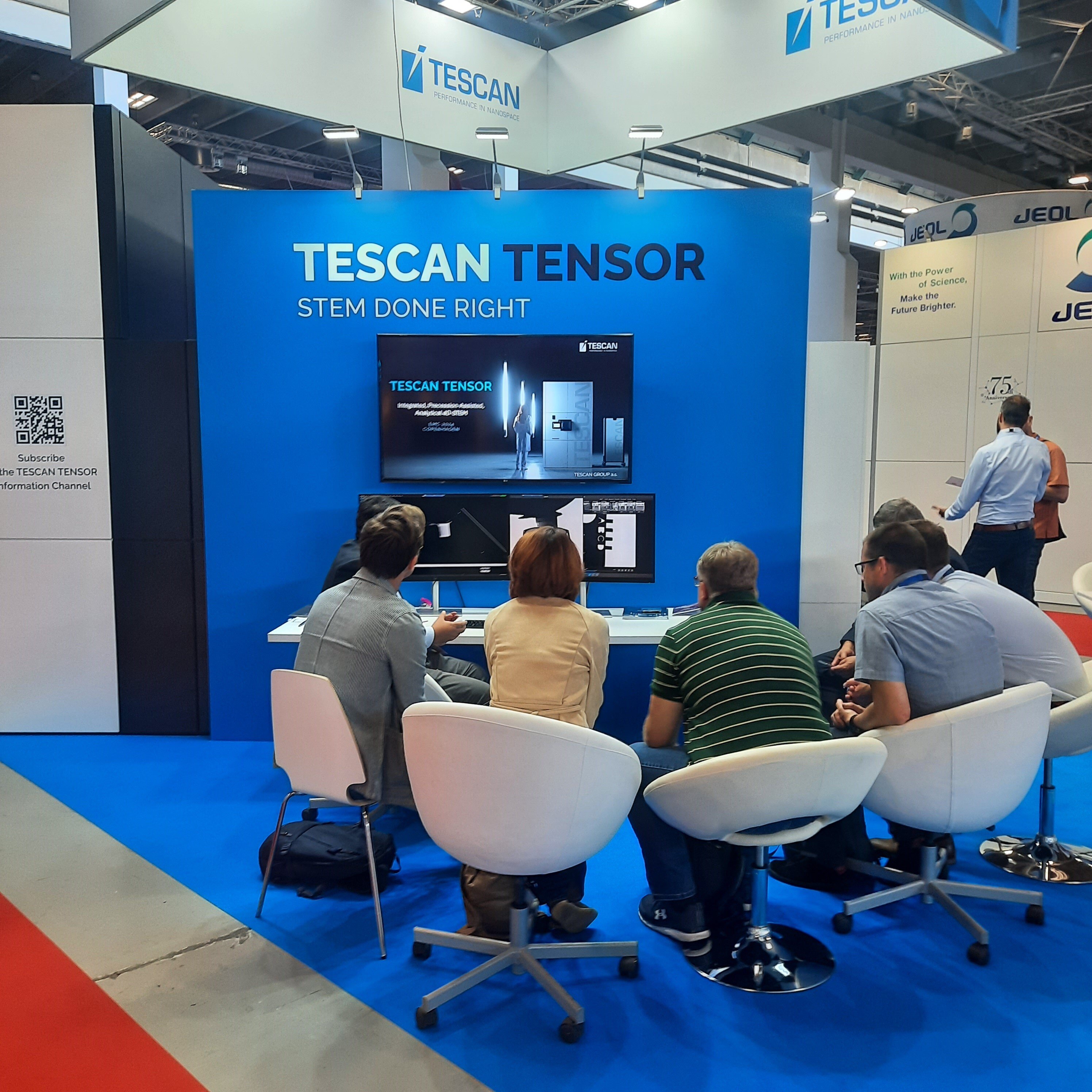
Analytical 4D-STEM for Everyone

TESCAN's 4D-STEM, redefining nanoscale multimodal characterization with synchronized diffraction imaging, EDS acquisition, beam blanking, and real-time data processing. TENSOR is as easy to use as an SEM — bringing true structural, morphological, and chemical analysis within reach of all researchers.

x
Register for a demo
x

TESCAN TENSOR

UniTOM-HR_tescan-1024x576 (1)

UniTOM HR

Real-Time Submicron 3D Imaging

The first dynamic micro-CT with true submicron resolution for non-destructive 3D imaging. See it in action and discover how UniTOM HR captures fine structural detail and supports advanced, in-situ materials characterization. A new standard in high-resolution, real-time micro-CT.

x
Register for a demo
x

TESCAN UniTOM HR

NANOSPACE by Orsay Physics

NanoSpace VR Experience

Configure the TESCAN UHV FIBs-SEM-SIMS in Virtual Reality

Experience the latest VR demonstration of NanoSpace. Put on the goggles and design your ideal UHV FIB-SEM. In this interactive VR station, you can explore the NanoSpace platform.

x
Register for a VR demo
x

NANOSPACE by Orsay Physics

Join Our Lunchtime Workshops and Poster Presentations


Workshop

Monday September 1
12:45 PM - 01:45 PM
2025-07-22_14-32-1

Proven to Lead: Automated FIB-SEM Workflows


When automation meets versatility. Learn how TESCAN’s automation simplifies FIB-SEM operations for new users, boosts lab productivity, and unlocks new application possibilities. Discover how unattended workflows, large-area analysis, and nanoscale prep all come together to elevate throughput.

Martin Slama photo
by Martin Sláma (TESCAN)
Conference Room 4
x

Micro CT

Registration form

Workshop

Tuesday September 2
12:45 PM - 01:45 PM
tensor banner

Boosting Productivity with Multimodal STEM


Analytical 4D-STEM for real labs. This session shows how TENSOR simplifies advanced STEM techniques — including 4D-STEM and 3D-ED — through fully integrated automation and intuitive data workflows. From defect analysis in alloys to beam-sensitive materials, see how you can achieve more in a single session.

Daniel Nemecek
by Daniel Němeček (TESCAN)
Conference Room 4
x

Micro CT

Registration form

Poster Presentation

Tuesday September 2
12:45 PM - 01:45 PM
gopi v1`-1

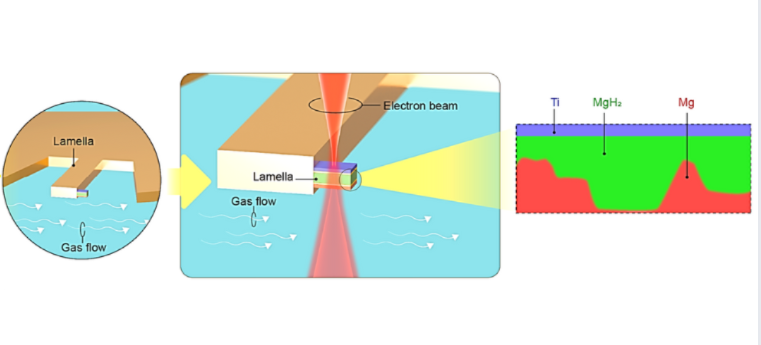
Unraveling metal hydride phase transformation mechanisms of Magnesium thin films using in situ/ex situ STEM EELS


The poster investigates how hydrogenation and dehydrogenation mechanisms in magnesium thin films are influenced by temperature, hydrogen pressure, and grain orientation, using in-situ and ex-situ STEM and EELS techniques. The study reveals distinct phase transformation behaviors under identical conditions, highlighting asymmetry in hydrogen storage kinetics.

photo
by Dr. Gopi Krishnan (Kongens Lyngby)
x

Micro CT

Registration form

Poster Presentation

Monday September 1
02:00 PM - 04:00 PM
Jana poster-1

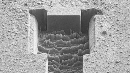
Employing Xe Plasma FIB for Fast and Precise Sample Preparation. 

Jana Šmídová
by Jana Šmídová (TESCAN)
Poster session 3, MC Karlsruhe, Germany
x

Micro CT

Registration form

Poster Presentation

Monday September 1
02:00 PM - 04:00 PM
martin poster-1

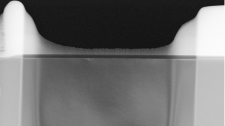
Influence of Applied Ion Energy on Low-Damage (S)TEM Sample Preparation Using Different Ion Species

Martin Slama photo
by Martin Sláma (TESCAN)
Poster session 3, MC Karlsruhe, Germany
x

Micro CT

Registration form

Poster Presentation

Tuesday September 2
02:00 PM - 04:00 PM
milos poster-1

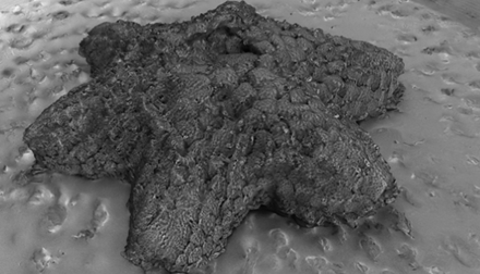
Application of Photogrammetry in SEM for High-Resolution 3D Reconstruction of Regions of Interest

Milos
by Miloš Hrabovský (TESCAN)
Poster session 9, MC Karlsruhe, Germany
x

Micro CT

Registration form

Schedule a meeting with our Sales and Marketing teams


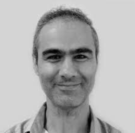
AXT - Kamran Khajehpour
I have been representing TESCAN in Australia and New Zealand for over 12 years, establishing the brand as a key player in the market. With a PhD in materials science from Monash University’s MCEM, I specialise in electron microscopy (SEM, FIB, TEM) and take pride in connecting researchers with TESCAN’s innovative solutions. I am passionate about advancing scientific research and value TESCAN’s user-focused approach to product development.
  • linkdin LinkedIn Profile
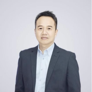
TESCAN – Sean Lee
TESCAN – Sean Lee
Currently as Managing Director of APAC region for TESCAN.  I have spend the last 30 years in the semiconductor and material analytical, metrology and inspection industry. Having served as an application engineer at Hitachi, Nikon, and business development role for Oxford Instruments (Plasma) and moved on with business leadership position at Nordson Corporation at Advance Technology and Electronic processing division in APAC region.
  • linkdin LinkedIn Profile
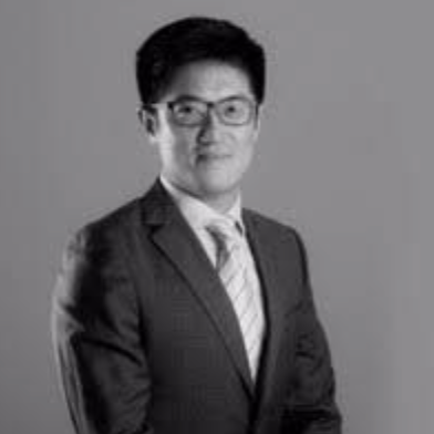
TESCAN – Yongkai Zhou

Dr. Yongkai Zhou had working experience with top 5 world EM producers and GlobalFoundries, taking various roles doing Electron Microscopy related businesses. He has vast experience in TEM, FIB, SEM, and MicroCT applications for materials science research and semiconductor failure analysis.

  • linkdin LinkedIn Profile
Image photo
ORSAY PHYSICS/TESCAN - Jéremie Silvent

Jérémie Silvent is the Sales Manager for Orsay Physics and Product Sales Leader for all the Orsay Physics products, including subsystems and OEM business. He is working for TESCAN Group since 2016. Before, Jérémie did multiple post-doctorate research projects where he specialized in cryo-SEM and cryo-FIB SEM.

  • linkdin LinkedIn Profile
TESCAN - Daniel Nemecek

Enthusiastic and experienced product and marketing manager of TEM/STEM microscopes with over 4-years of experience managing mid-range TEM products from market analysis to product conception, development and release.

  • linkdin LinkedIn Profile
TESCAN - Martin Slama

Product marketing manager for FIB-SEM 3D characterization and TEM lamela preparation in Materials science with over 8 years experienceworking with FIB-SEM instruments.

  • linkdin LinkedIn Profile
TESCAN - Lucie Hofrova

Lucie (Customer Solutions Specialist) brings rich customer service experience, mainly from the area of logistics and planning. Her main responsibility is service-product management.

image002
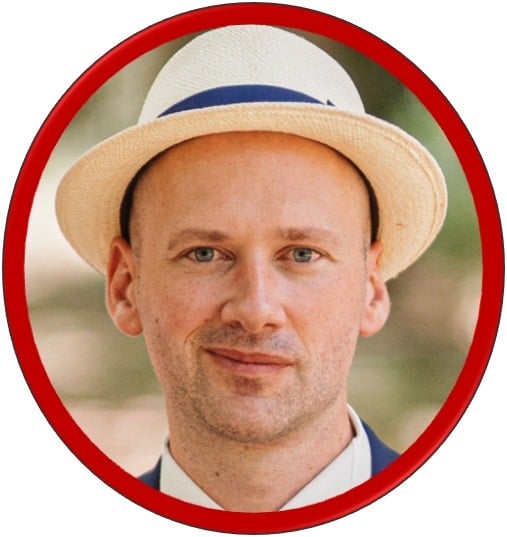
Dirk van der Wal, Chief Marketing Officer

Dirk van der Wal is acting Chief Marketing Officer, and Liaison Officer for TESCAN White Label partners in Japan and China. His experience includes applications, product management and product marketing of charged particle optics instruments (SEM, STEM, FIB and micro-CT), primarily in the fields of Materials Science incl. Batteries, Geosciences, and Process Mineralogy (Automated Mineralogy).

  • LinkedIn Profile

Aura Gentle Ion Beam™


Achieve pristine lamella quality


Post-FIB low-energy Ar⁺ polishing (as low as 200 eV) removes Ga-implanted layers, eliminates surface contamination, and reveals atomic-level structure clarity.


GIB-1


OptiGIS O₂


Smarter milling for carbon-based materials


Inject oxygen during patterning to boost etch rates up to 50%, reduce carbon redeposition, and improve contrast in polymers, resins, and diamond substrates.


Opti GIS-1


TEM AutoPrep Pro


High-quality lamellas


Fully automated inverted and planar lift-out workflows and robust failure-handling. Even novice users can prepare thin TEM samples with confidence.


tem 3


AutoSection


Cross-sectioning on autopilot


Automate cross-sectioning across multiple areas and samples with enhanced surface quality and higher throughput. AutoSection combines rocking polish automation, intelligent image-based navigation, and overnight batch scheduling to maximize your lab’s productivity and reproducibility.


auto3


Find Us at Karlsruhe, Messeallee 1, 76287 Rheinstetten, Germany 

Can't Attend MC 2025? Let’s Stay in Touch


If you are unable to attend this conference, we will be happy to contact you, if you have any questions or requests.

Glimpses from Past Global TESCAN Events